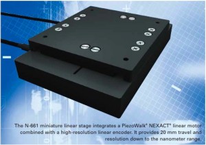
We soon will be expanding the positioning and resolution capabilities of the photon factory by installing an additional X-Y stage from Physik Instrumente (PI). The stage uses PI’s patented NEXACT PiezoWalk technology to achieve high resolution and long travel distances:
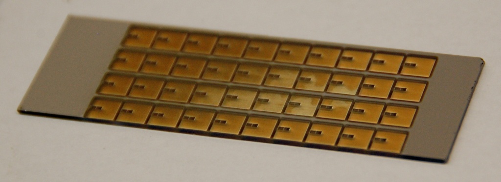
An array of interdigitated electrode masks in chrome on glass.
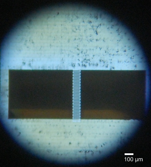
The photo to the left shows the creation of a positive lithography mask, cut using the PF µ-machining system by Cosmin Laslua.The photo illustrates our first attempt to create a new process. Namely, large area removal of a thin film with the excimer laser system. The light brown discoloration shows evidence of a residual chrome dust on the surface of the glass. We are currently investigating ways to improve this process and more thoroughly remove the residual metal. We think this can be accomplished through the addition of processing gas to our µ-machining system or with post machining chemical etch methods available in the new UA microfab. The photo below shows the fidelity of the laser cutting process. The laser cut interdigitated electrodes have a width of only ~ 5 µm. This represents a 1000:1 scale difference between these channels and the the largest (5mm) features in the above picture. This was accomplished with a multilayer CAD drawing and a realignment of the PFµM cutting mask size. You can also see the residual chrome dust coloring the above image in the cleared 5mm x 5mm regions.
5 µm interdigitated electrodes cut with the PF laser µ-machining system.